
SEMICON West 2014 in San Francisco was a great place to meet bloggers in the semiconductor industry to get updated on the status of 450mm diameter silicon wafers. On one side, there is a good news about the unprecedented level of collaboration taking place between the design and construction professionals through the Global 450mm Consortium (G450C) to deconstruct a semiconductor facility matter associated with 450mm adoption. But on the other hand, the transition to 450mm seems delayed till 2020 with Intel and TSMC backing off their timing for introduction of 450mm in volume production.
An analysis of the macroeconomics of this capital intensive microelectronics business and its impact to macroeconomic growth of U.S. economy shows that 450mm diameter silicon wafers need to be introduced sooner rather than later to keep this business profitable and for sustaining the macroeconomic growth. This article presents an analysis of the macroeconomics of manufacturing 450mm diameter wafers, how it would help in sustaining progress of Moore’s Law and what precautions need to be adopted by semiconductor industry at G450C to ensure a sustainability of huge capital investments for transitioning to 450mm diameter wafers.
The global semiconductor industry has been constantly increasing the diameter of the silicon wafers it uses to reduce its manufacturing costs through mass production. The larger the diameter of wafers, the more real estate of silicon that is available for manufacturing. The increasing process complexities in nanoscale engineering add to silicon manufacturing costs. However, if the percentage increase in manufacturing costs per wafer from advancements in technology is smaller than percentage increase in revenue from the larger real estate of silicon, then the semiconductor manufacturing business becomes profitable.
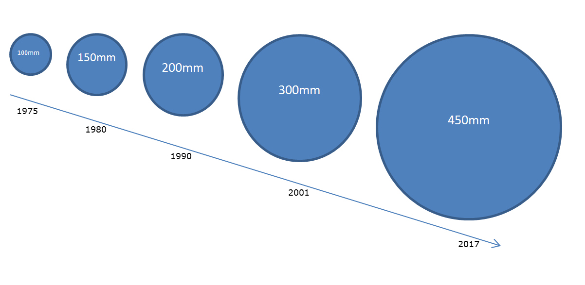
At present, the semiconductor industry is widely making use of 300mm diameter wafers, and there is some progress towards 450mm diameter wafers, but major players are delaying their investments for 450mm diameter wafers due to significantly high manufacturing costs of semiconductor processing tools and lower expected returns on investments. The major players in this business do not expect to reap significant returns from their huge capital investments which is raising questions whether mass production of 450mm diameter wafers would even become a reality anytime in near future.
Whenever a new wafer size is first introduced, the cost per square inch of silicon on a given wafer size is at its peak. But, as the technology matures, this cost per square inch drops with time. The minimum silicon cost reached with 125mm diameter wafers is about US$ 1 per square inch. The minimum silicon cost with 200mm diameter wafers is about $2 per square inch, resulting in a maximum cost per wafer of $100.. The minimum silicon cost reached with 300mm diameter wafers is about $3 per square inch, resulting in a maximum cost per wafer to of $400. Thus, for every succeeding increase in wafer size, there is approximately a 1.4 times increase in costs of manufacturing.
The silicon wafers that are used for manufacture are sliced from a silicon ingot, which is approximately 99.99999 percent pure silicon. The increases in cost per square inch occurs due to other reasons, such as the percentage of wafer that actually goes into the product, actual consumption of these wafers, and the research and development costs involved in the manufacture of wafers. Because of increasing processing complexities in subsequent generations of increased wafer size, the thickness of the wafers sliced from silicon ingots is larger. Thus, the total number of wafers that can be sliced from a silicon ingot decreases with increasing wafer sizes.
Additionally, the actual silicon going into the wafers is a small percentage of the total silicon available for use from these silicon ingots. According to Rose Associates, this percentage was 30 percent for 150mm wafers, 17 percent for 200mm wafers, and close to 10 percent for 300mm wafers. Based on this trend, the percentage of actual silicon from ingots that would go into use for 450mm wafers would be even lower than 10 percent, possibly closer to 5 percent, based on the observed trend. Thus, the actual silicon from ingots going into electronic products is progressively decreasing for every generation of increase in silicon wafer size. A larger wafer size also increases the number of chips that are mass produced.
The above data analysis educates us that for ensuring a sustainability of huge capital investments towards a transition to 450mm diameter wafers, the majority of silicon that is manufactured inside a semiconductor wafer fab should get consumed in the manufacture of electronic products. Now the question is how does semiconductor industry make it feasible? A good consumption of manufactured silicon can be achieved only when there is a robust economic demand for latest and greatest electronic products. Hence, the G450C consortium should not only ensure reduction in costs of manufacture to ensure sustainability of production but should also collaborate to ensure that there is good consumption of its manufactured products. This can be made possible only in an economy where the consumers have a higher purchasing capacity to generate a robust demand for semiconductor products.
The Global 450 Consortium (G450C), a New York-based public/private program with leadership from GlobalFoundries, IBM, Intel, Samsung, TSMC, and the College of Nanoscale Science and Engineering (CNSE), is housed on State University of New York’s (SUNY’s) University at Albany campus and maintains focus on 450mm process and equipment development. In this consortium, there is an unprecedented collaboration and cooperation between previous competitors in such a way that:
•All key players are coming together
•CNSE is providing a uniquely neutral and technologically advanced home for critical research
•Work of the G450C is being guided by a strict application of an inside-out design approach
•Key advances have been made in utility requirements, overhead conveyance systems, and energy efficient strategies.
This collaboration is first step forward by the global semiconductor industry to ensure a steady supply of 450mm diameter silicon wafers at a reduced cost. However, unless this consortium also ensures a similar collaboration and cooperation to generate a steady demand for this newly manufactured silicon, the huge capital investments made by the participants in the G450C consortium towards a transition to 450mm diameter silicon wafers cannot become sustainable.
On the macroeconomic side for U.S. economy, the consumer purchasing power of majority in the U.S. economy has shrunk because of the transformation of U.S. economy from a free market enterprise to monopoly capitalism. As a result of this, there is a growing gap between the wages and the productivity of employees in the U.S. and global economy, which is resulting into a loss of economic balance. When capitalism is reformed to a free market enterprise, and it works for all citizens in an economy, it would usher in an economic democracy. As it would work for all citizens, monopoly capitalism will become mass capitalism.
In order to sustain the progress of semiconductor industry which has been driven by the relentless progress of Moore’s Law, macroeconomic reforms have become critical to allow semiconductor companies to justify their ever-increasing capital-intensive investments for transitioning to 450mm diameter wafers. By establishing free markets, supply and demand of electronic goods would grow in proportion, thereby resulting in a balanced economic growth, low income taxes on individuals, higher investments, increased motivation for employees to work hard, and the growth of the overall economy. These free market reforms seems to be the only path forward for global semiconductor industry to ensure its sustainability for transition to 450mm diameter silicon wafers.
When the G450C consortium collaborates to bring about such profound macroeconomic reforms, even if the future improvements in process technology for progress of Moore’s law are less from one process generation to another, the macroeconomic growth in the overall economy would be very high. These reforms would ensure that the consumer purchasing power and hence prosperity of overall economy would be very high. With a high economic demand, the demand for the latest and greatest electronic products will continue to grow. In this way, the G450C consortium can ensure a good consumption of all manufactured silicon from larger size of 450mm diameter wafers. This robust consumer demand would force semiconductor industry to make more investments and manufacture latest and greatest electronic products to meet that growing demand.
In this way, mass capitalism based free market reforms envision sustainability of huge capital investments in the transition to 450mm diameter silicon wafers. Looking back into the history of macroeconomics, it can be observed that an economic depression might occur when money that is in the possession of individuals stops rolling. Some of major players in global semiconductor business are concerned that their investments for transitioning to 450mm diameter wafers would not give any significant returns. This could turn out to be one of the causes for money to remain inert or unutilized in this capital intensive business.
As a result of above policies, money in the economy would become immobile or inert; consequently, there would be no investment, no production, no income and hence further reduction in consumer purchasing power. The situation could become so dangerous that there would be very few buyers to buy new electronic goods. This macroeconomic analysis explains why macroeconomic reforms have become critical for transition to 450mm diameter silicon wafers to ensure that money does not remain inert and it keeps circulating in the economy in order to keep increasing the consumer demand for the latest and greatest electronic products. Without above proposed macroeconomic reforms, progress of Moore’s law seems impossible and chances of the U.S. economy transitioning from a great recession to a depression seems inevitable.
Recent Comments